Circuit diagram of boost converter From Fig. 3, during the switch
€ 35.50 · 5 (302) · Auf Lager

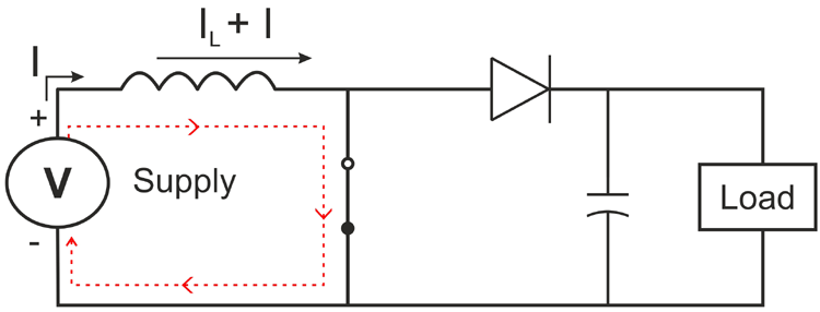
Download scientific diagram | Circuit diagram of boost converter From Fig. 3, during the switch is closed [10]; Vs is constant supply voltage, Vs = VL= L × (di/dt) (5) During the switch S is open; VS = VL + VC (6) Then, L × (di /dt) = VS-VC; di/dt = (VS-VC) / L Current increment when switch closed for duty cycle D; Imax-Imin = (VS /L) × D×T (7) Current decrement when switch open, Imin-Imax = (VS-VC) / L × (1−D) ×T (8) from publication: Performance of closed loop SEPIC converter with DC-DC converter for solar energy system | The Non-Conventional sources such as solar energy has been replacement and best exploited electric source. The solar electric power required DC-DC converter for production, controllable and regulation of variable solar electric energy. The single ended boost converter has | DC-DC Converters, Solar Energy and Solar | ResearchGate, the professional network for scientists.

Figure 3 from Small-signal modeling of the PWM boost DC-DC
Simple Buck-Boost Converter Circuits Explained - Homemade Circuit

Circuit diagram of Cuk Converter From Fig. 4, when Switch S is

DC Boost Converters; Testing with Variable Input and Duty Ratio
Circuit diagram of the boost converter.
Stability Analysis of Feedback Loops Part Two

Circuit diagram of Boost converter.

Figure 3 from A switched inductor multilevel boost converter

Circuit diagram of boost converter From Fig. 3, during the switch

Step-up (boost) converter (a) equivalent circuit, (b) equivalent